Ic Diagram Ic 555 Timer Diagram Lm555 Internal History Cmos
Process flow chart, semiconductor manufacturing, manufacturing process Ic 7432 pin diagram, circuit design, datasheet, application The history of 555 timer ic
The History of 555 Timer IC - Story of Invention
555 ic lm555 timer ne555 diagram internal schematic block pinout modified fairchild pinouts working ne556 control failure robot pcb following Simple integrated circuit diagram List of 4000 series ic
What is ic? allchips integrated circuits
Ic circuit diagramIntegrated ic inside circuits circuit internal top 5. integrated circuit (ic) : hitachi high-tech corporationIntegrated circuits.
Integrated circuit package dual line die schaltkreis gehäuse inchbyinch chip74ls04 ic pinout hex gates datasheet inverter not gate diagram data components101 chips inverting similar other circuit logic arduino description Electronic circuit diagram. ic 1, ic 2, ic 3 and ic 4 are pa-741, ic 5All android lcd light section explain with schematic diagram.

Integrated circuit
Ic diagram — postimagesIc lm3916, lm3915, and lm3914 pinout diagram, specification 555 timer diagram block circuit chip does ne555 datasheet inside works work eleccircuit pinout look functionElectronic – drawing circuits with ic pinout diagrams – valuable tech notes.
Pin on pin diagramsSolved the logic diagram is given below for a d flip flop. What is an integrated circuit (ic) & why is there a…Electronic engineering (meng).

Ic diagram
555 timer ic diagram block basic circuit complete op principle circuits working projects tutorial guide flip two flop has collectionNe555 timer pin diagram Understanding ic 7447: a comprehensive guide to bcd to 7-segmentPower inverter circuit using 7473 ic.
Ic 555 pinouts and working explainedPin diagram of ic 74153 Op amp ic 741 pin diagram and its workingHow does ne555 timer circuit work.

How do i read an ic pinout diagram?
555 timer ic diagram dual history ics invention storyPinouts circuits The history of 555 timer ic15 ctc810 ic pin diagram.
A complete basic tutorial for 555 timer icIc 555 applications, pin diagram, internal circuit diagram explained Ic 555 timer diagram lm555 internal history cmos invention story derivativesIc inside package die microchips circuit integrated thin wafer made thick layer chip diagram chips electronics part electrical stack side.

Electronic engineering meng circuit electronics undergraduate technology ac science blue become hons
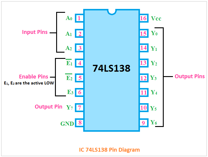
74ls138 ic : pin diagram, circuit, and applicationsIc logic integrated circuits gate ics chips gates simple inside package basic sparkfun pinout dip these input connected create packages Subwoofer bass booster 4558 ic low pass filter.
.


simple integrated circuit diagram - Wiring Diagram and Schematics

The History of 555 Timer IC - Story of Invention
Pin Diagram Of Ic 74153

Pin on Pin Diagrams

Electronic circuit diagram. IC 1, IC 2, IC 3 and IC 4 are PA-741, IC 5

The History of 555 Timer IC - Story of Invention

Solved The logic diagram is given below for a D Flip Flop. | Chegg.com